Nanopositioners can provide high-precision, repeatable motion with nanometer or sub-nanometer resolution. These devices are used as an integral component in numerous scientific and technological applications. Nowadays, the growing need for precise positioning, manipulation, and interrogation of matter in the micro to nanoscale range is a significant driver for developing fast and highly-accurate nanopositioners.
Microelectrothermal systems (MEMS) have recently emerged as an alternative approach for the realization of nanopositioning platforms. The small size, low fabrication cost and fast dynamics of MEMS nanopositioners have led to them being considered for applications such as probe-based data storage and on-chip atomic force microscopy. LDCN has developed a series of novel MEMS nanopositioners whose intended use is as a scanner within an atomic force microscope (AFM). By miniaturizing one of the AFM's major components, this is an important step towards the development of a fully microfabricated AFM.
For imaging, the MEMS nanopositioners are implemented as the scanner for the AFM, with its built-in scanner being bypassed. Closed-loop controllers are designed to allow them to accurately track a reference trajectory and therefore make AFM imaging possible. In addition to implementing a conventional raster scanning method to generate AFM images with the MEMS nanopositioners, non-raster scanning methods such as Lissajous scanning and spiral scanning have also been demonstrated.


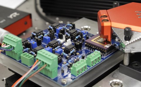
Left: The test set-up where the packaged MEMS device is being used as an in-plane scanner for an AFM. The custom-made PCB provides the sensing and actuation circuits.
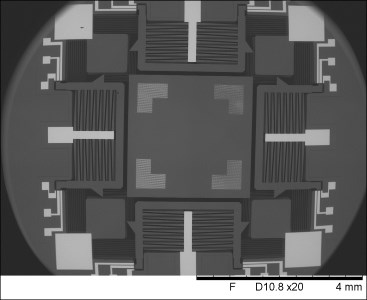
Right: A parallel kinematic 2-DOF MEMS nanopositioner with a bandwidth of above 4.4 kHz along each axis. Electrostatic actuators are used to achieve an in-plane displacement range of about ±5 μm, while electrothermal sensors are implemented that provide a measurement resolution of a few nanometers. The design, control, and use of the device for AFM imaging are explained in IEEE Transactions on Control Systems Technology. A raster scan with a maximum frequency of 800 Hz is implemented for this device.


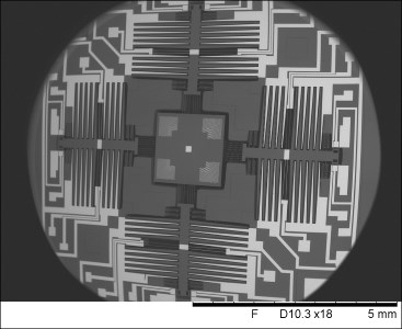
Left: A parallel kinematic 2-DOF MEMS nanopositioner with electrostatic actuators providing a large displacement range of more than 20 μm along each axis. Electrothermal sensors are also implemented for real-time displacement sensing. The device is used for AFM imaging using the Lissajous scan method, as reported in Review of Scientific Instruments. The use of spiral scanning for AFM imaging with this nanopositioner is reported in IEEE Transactions on Control Systems Technology.
Right: As opposed to the use of a parallel kinematic mechanism, a serial kinematic mechanism is can also implemented in the design of a 2-DOF MEMS nanopositioner. The problem of signal routing to the inner stage is solved using a suspended substrate configuration, as described in IEEE Journal of Microelectromechanical Systems.


Left: Electrothermal sensors are commonly used in MEMS nanopositioners to measure in-plane displacements. The sensor comprises two heaters whose temperatures change in a differential manner as a heat sink moves in front of them. The change in the heaters’ temperature induces an opposite variation in the electrical resistance of the heaters, which can be translated to an output voltage. Electrothermal sensors have a small form factor while being able to provide a nanometer-range sensing resolution. However, the sensing bandwidth of these sensors is relatively limited.
Right: A novel displacement sensing method is proposed which exploits the bulk piezoresistivity of silicon in a differential configuration. Using this method, there is no need to implement highly-doped regions on silicon, while the sensor shows a wide measurement bandwidth and practically zero footprint. The sensor is incorporated here in a 2-DOF MEMS nanopositioner. The nanopositioner demonstrates a displacement range larger than 15 μm and in-plane resonance modes above 3.6 kHz in both axes. Sensing bandwidths as wide as 55 kHz are experimentally demonstrated for the piezoresistive sensors. The design and characterization of the device are reported in IEEE Sensors Journal.